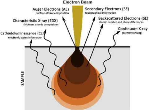
Electron microscopy utilizes electromagnetic lenses to focus electron “light” waves to resolve features on material surfaces, the spatial resolution is related to the energy (higher energy, better spatial resolution). The technique requires that samples be vacuum compatible so that the “particles” of electrons do not interact with the atoms in the air.
A scanning electron microscope (SEM) rasters the electron beam across the sample surface for imaging. Images are acquired by detectors from a variety of signals that emerge when the electron interacts with the sample. Each type of signal emerges from different volumes of the sample, which limits the spatial resolution of the technique.
SEM can be coupled with a focused ion beam (FIB) source to enable micro/nano-machining. The dual-beam SEM-FIB has revolutionized the sample preparation of thin-foils needed for transmission electron microscopy (even higher spatial resolution), and also allows researchers to conduct serial sectioning to interpret 3D assemblies of microstructural information.
This is a 3D rendering of the grain boundary network measured by serial sectioning in a FIB-SEM. The grain boundaries in nickel-based superalloys are "bumpy" because of the high volume fraction of secondary particles that are responsible for their very unique high-temperature properties. data collected and shared in DOI: 10.1016/j.msea.2015.05.031
Transmission electron microscopy (TEM) has increased spatial resolution compared to scanning electron microscopy but requires that samples be electron translucent so that the detectors, placed below the sample, can acquire signals that are transmitted through the sample. The technique achieves higher spatial resolution because 1) it uses higher energy, lower wavelength, electron source and 2) the thin foils artificially reduce the interaction volume between the electron source and the sample. The combination of these two reasons means that this technique can sometimes produce data at angstrom-level spatial resolution.
In the Swagelok Center for Surface Analysis of Materials at Case Western Reserve University, we maintain and train students on both an SEM system (ThermoFisher Apreo 2S) and a dual-beam SEM-FIB (FEI Helios NanoLab 650) for imaging and micro-fabrication of samples. SCSAM maintains a remote link to four TEMs at The Ohio State University. Users interested in training should contact the SCSAM executive director.

